ANDREW J. HAIDINYAK
——————
APRIL 2026
PRIOR ART
DOCUMENTED
——————
ALL RIGHTS
RESERVED
Strike Cruiser-Class Graphics Platform
Created by: ANDREW J. HAIDINYAK — HBlockAndrew.com
Prior Art Documentation — April 2026
Independent Engineering Concept
Full Technical & Business Analysis
PHAETON is an independent board-level GPU architecture concept that uses three power-capped RTX 5080-class GB203 dies, coordinated through high-speed interconnect and hardware synchronization, to explore a practical path beyond the thermal, power, and yield limits of monolithic flagship graphics cards.
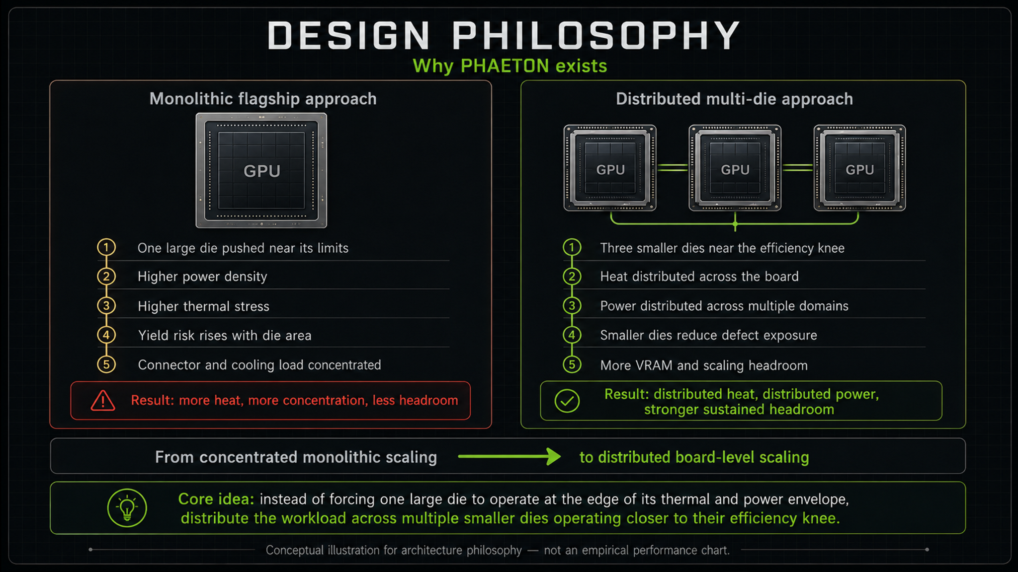
The concept is built around one central idea: instead of forcing one large die to operate near the edge of its power and thermal envelope, distribute the workload across three smaller dies operating closer to their efficiency knee. The result is a proposed graphics platform designed for higher sustained performance, lower thermal stress, greater VRAM headroom, and stronger long-term reliability — at a price point that makes sense for consumers, developers, and NVIDIA.
This project is an independent engineering concept study and prior-art documentation. It is not affiliated with, sponsored by, endorsed by, or associated with NVIDIA Corporation. All trademarks, product names, and company names are the property of their respective owners. Performance, cost, thermal, and business figures are modeled estimates unless otherwise stated.
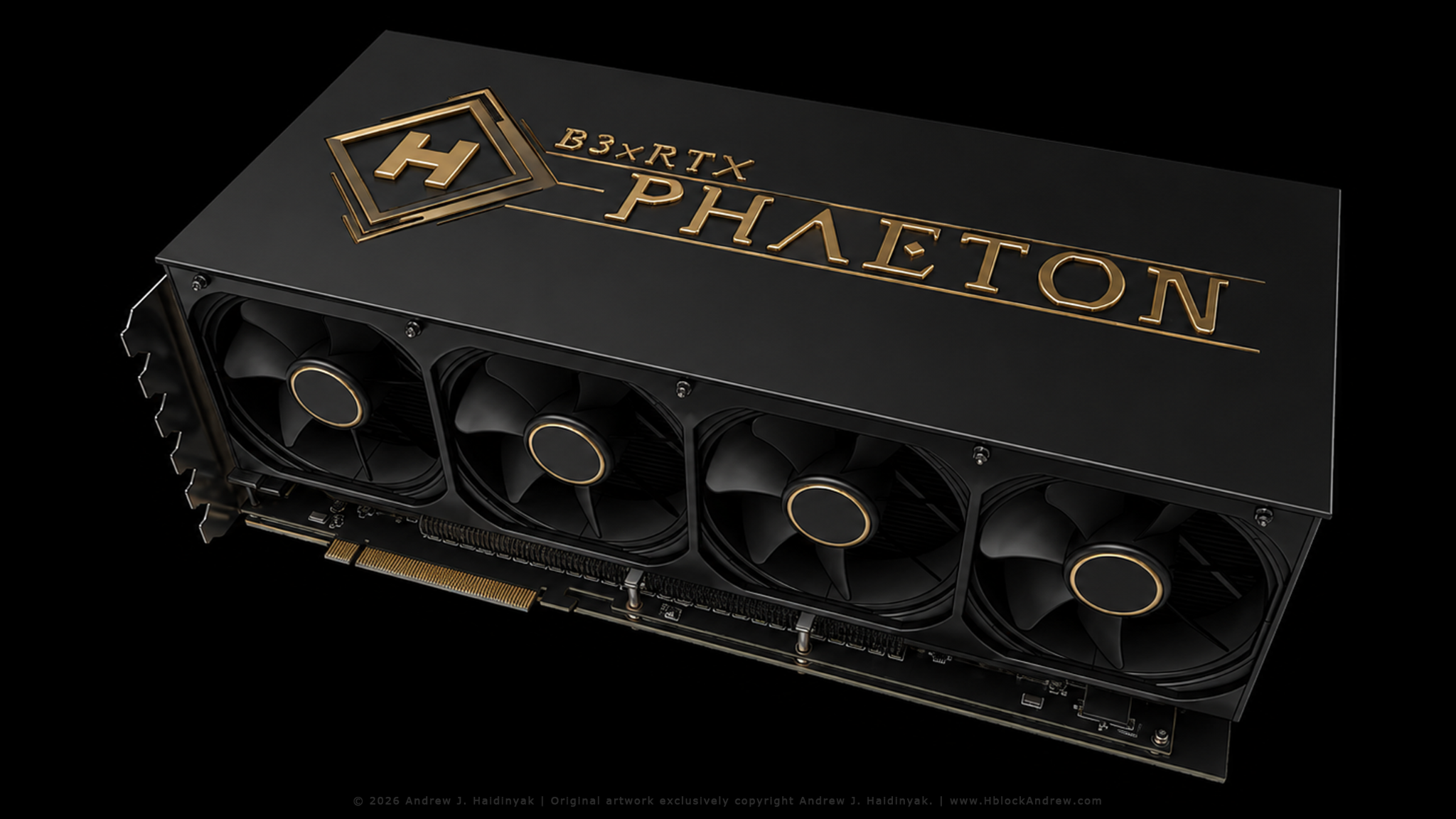
& DISCLOSURE
Why this concept exists
The gaming market built NVIDIA, but the next stage of performance scaling may not come from pushing a single flagship die harder. As power density, thermals, connector load, die yield, and memory demand continue to rise, the stronger path may be distributing the workload across multiple smaller dies operating closer to their efficiency knee. PHAETON exists to explore that path: a board-level architecture designed around distributed heat, distributed power, distributed memory capacity, and hardware-assisted synchronization.
Every GPU die has an efficiency knee — a range where performance per watt is strongest before voltage, heat, and leakage begin producing diminishing returns. PHAETON is built around the idea that three smaller dies operating closer to that efficient range can deliver stronger sustained performance than one large die pushed near the edge of its thermal and power envelope.
Large monolithic dies are expensive because yield risk rises with die area. Smaller dies generally produce more usable chips per wafer and reduce the financial impact of defects. Under PHAETON's stated assumptions, three GB203-class dies can provide a stronger balance of silicon cost, compute density, and manufacturing flexibility than one larger flagship die.
The consumer value is simple: one card, one platform, 4K native, more VRAM headroom, lower thermal stress, and a longer usable lifespan. PHAETON is designed for gamers, creators, developers, and small studios who need flagship-class performance without turning every purchase decision into a power, cooling, and memory-capacity compromise.
The RTX 5090 is the flagship
How do you build a strike cruiser capable of surpassing a flagship? First, identify its weaknesses. Power. Thermals. Noise. Scalability — this is where even a flagship reveals its vulnerabilities.
Modern flagship GPUs are extraordinary pieces of engineering, but the monolithic approach is beginning to concentrate too much power, heat, mechanical load, and yield risk into a single package. As die area, board power, memory demand, and cooler mass increase, the margin for error becomes smaller: connector load rises, heat flux becomes harder to manage, shipping stress becomes more severe, and thermal cycling places greater strain on solder joints over time.
PHAETON starts by identifying these pressure points. The goal is not to dismiss the monolithic flagship model, but to show where its scaling path becomes increasingly difficult — and where a distributed multi-die board architecture may offer a cleaner engineering tradeoff.
A single 16-pin PCIe power connector is rated for up to 600W. The RTX 5090 draws up to 575W — 95.8% of that rating. Increased contact resistance from incomplete seating, cable quality, connector wear, or installation variance can raise local temperatures and increase the risk of cable or connector damage. System-side power quality may further reduce operating margin when poor PSU transient behavior, voltage instability, or degraded input power is introduced.
As board power rises, the architecture becomes less tolerant of those variations. A design with greater electrical headroom can absorb more real-world inconsistency before small system-side problems become thermal, stability, or reliability problems.
— Andrew J. Haidinyak · PHAETON · April 2026
- Design-origin risk — operating close to the connector's rated capacity leaves limited tolerance for cable resistance, installation variance, and sustained high-current load.
- User-handling failures — improperly seated connectors, aftermarket cables, inadequate airflow. Difficult to prove at return; these cases can still create support and replacement costs when root cause is difficult to establish.
- Shipping & installation damage — a 1,100g+ card in a consumer box, often installed and uninstalled multiple times. PCIe slot stress, solder joint fatigue from transit shock, broken shroud clips.
The corresponding modeled warranty reserve is approximately $24.92 per RTX 5090 shipped and $20.44 per PHAETON shipped. Applied to modeled direct contribution, this reduces the RTX 5090 from approximately $1,114 to $1,089 per unit and PHAETON from approximately $1,309 to $1,289 per unit.
The difference is not that every returned card incurs the full cost of a replacement. The model spreads expected warranty cost across all units shipped. PHAETON's lower modeled return rate offsets its higher per-event replacement cost, leaving an expected warranty reserve of approximately $20.44 per unit versus $24.92 for the RTX 5090. After that reserve, PHAETON retains approximately $200 more modeled direct contribution per unit.
$20.44 expected warranty reserve per unit shipped
The Phaeton solution is an entirely new class of graphics card: the Strike Cruiser
PHAETON does not answer the limits of flagship scaling by building an even larger monolithic GPU. It proposes a different system architecture entirely: a coordinated multi-GPU platform built around three power-capped GB203-class dies operating on a single board, supported by distributed power delivery, oversized air cooling, hardware-assisted synchronization, and a rigid structural frame. This is not an incremental step forward. It is a fundamental shift in how a high-performance graphics platform can be built.
The objective extends beyond performance and thermals. PHAETON is designed to distribute the pressures that increasingly concentrate inside modern flagship GPUs. Compute is divided across multiple dies. Heat is spread across a much larger physical area. Input power is shared across two primary connectors. Mechanical load is transferred away from the PCB and into a reinforced frame and external support system. By leveraging standardized, readily available dies in a coordinated multi-chip configuration, the architecture redistributes computational load, electrical demand, and thermal stress across the platform. Key failure modes were identified and designed against before a single component was placed. The result is not simply more hardware on one board. It is a more balanced machine.
PHAETON represents the first generation of a potential new class of GPU architecture, designed to explore performance beyond the practical limits of today's monolithic designs while the next generation of manufacturing, packaging, and interconnect technologies matures.
That headroom is intended to reduce the airflow and fan speed required during sustained gaming loads. Final temperatures and acoustic performance would require CFD, prototype instrumentation, and thermal validation.
The dual-input architecture is intended to reduce current concentration and improve tolerance for contact resistance, cable variation, and sustained high-load operation. It does not remove the need for correct connector seating, cable quality, PSU capability, or power-delivery validation.
VS ~4% FOR RTX 5090
The objective is to reduce board flex, protect large BGA packages, and improve resistance to shipping and installation stress. Final effectiveness would require mechanical simulation, drop testing, and production chassis validation.
The proposed installation system combines a reinforced card frame with a floor-mounted support structure or chassis-integrated mounting point that transfers most of the card's static weight away from the PCIe connector and motherboard slot. The goal is to reduce long-term cantilever stress, limit vibration, improve shipping stability, and protect the PCB and large BGA packages from unnecessary mechanical loading.
Under the stated thermal assumptions, each die is projected to operate at lower temperature and lower heat flux than a single heavily loaded flagship die. Reduced operating temperature and thermal swing may also improve long-term package and solder-joint reliability.
Current acoustic and temperature figures are modeled targets, not measured prototype results. Final performance would depend on shroud restriction, fin pressure drop, fan interaction, case airflow, bearing noise, and system-level resonance.
The production goal is for software to interact with the board as one coordinated graphics device. Whether the full 48GB can behave as a practical unified addressable pool for all workloads depends on driver architecture, memory-management policy, inter-die latency, and application support.
The theoretical compute capacity of a two-die configuration is approximately 67% of the full three-die system, although real degraded-mode performance would depend on workload redistribution, memory availability, driver behavior, interconnect health, and the location of the fault.
For professional users, time is money. A conventional GPU failure can stop a workstation completely. PHAETON is designed around a different possibility: keep moving forward on the battlefield. Even at reduced capacity, the system may be able to finish a render, preserve a development schedule, complete a critical workload, or remain productive until replacement hardware arrives.
The objective is not fault immunity. It is operational resilience.
RTX 5080 — GB203 die
GB203 is the foundation of PHAETON because it occupies the middle ground the architecture requires: substantial Blackwell-class compute, a native 256-bit GDDR7 interface, manageable die size, and an operating range that can be power-capped without sacrificing the entire performance envelope.
PHAETON does not use three GB203-class dies simply to multiply core count. The architectural argument is that a smaller die operated closer to its efficiency knee can become more valuable when compute, heat, power delivery, and memory capacity are distributed across the board. Section 05 establishes the building block. The sections that follow explain how three of those building blocks are intended to operate as one coordinated platform.
128 per SM
256-bit GDDR7
AT STOCK BOOST
PHAETON uses three different compute figures depending on the operating condition being discussed. ~171 TFLOPS — THEORETICAL STOCK AGGREGATE refers to the combined theoretical stock FP32 throughput of three GB203-class dies. ~162 TFLOPS — MODELED PHYSICAL TARGET · 3×300W refers to the modeled aggregate physical throughput at PHAETON’s approximately 300W-per-die operating target. ~138–146 TFLOPS — MODELED EFFECTIVE-EQUIVALENT represents the modeled range after an estimated 10–15% coordination and synchronization overhead.
Unless otherwise stated, all performance figures in this document should be read within those defined operating conditions. Theoretical aggregate throughput describes the installed compute capability of the hardware; modeled physical throughput reflects the proposed power-capped operating point; effective-equivalent throughput accounts for estimated multi-domain coordination losses in real workloads.
The GB203 die uses a 256-bit GDDR7 memory interface. In the standard eight-device configuration, each memory device contributes 32 bits, giving 256 ÷ 32 = 8 devices per die. Across three GB203-class subsystems, the platform therefore uses 24 GDDR7 devices and provides 48GB of total installed memory capacity. Each die retains its own 256-bit interface and up to 960 GB/s of local memory bandwidth, producing 2.88 TB/s of aggregate physical memory-interface bandwidth across the complete three-die platform. That 2.88 TB/s figure should not be interpreted as universally available unified bandwidth. Effective cross-domain memory performance depends on interconnect bandwidth, data placement, memory-management policy, driver architecture, and workload behavior.
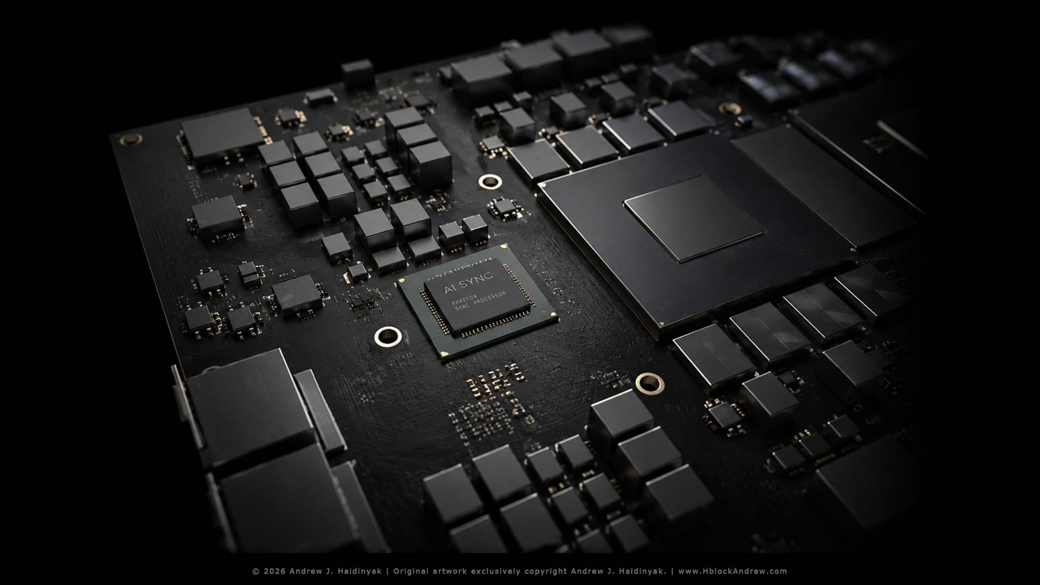
AI Synchronization Controller — Beyond Traditional SLI
PHAETON does not rely on traditional SLI. Instead, it proposes a board-level multi-die graphics architecture where three GB203 dies operate as coordinated rendering domains under a central AI Synchronization Controller.
Each die is assigned a primary workload domain — geometry and rasterization, shading and lighting, or ray tracing and compute — while the driver and runtime remain responsible for workload policy, resource allocation, memory placement, domain assignment, and redistribution when one domain becomes the limiting stage. The domains are therefore adaptive rather than permanently fixed.
The AI Synchronization Controller does not replace the game engine, driver, runtime, or native GPU schedulers. Its role is narrower and more specialized: it monitors timing, dependency, queue-state, and utilization telemetry from the three GPU domains and uses that information to help coordinate synchronization points, workload handoffs, transfer windows, frame timing, and output pacing. Conceptually, the AI Synchronization Controller acts as "The Juggler" — continuously watching three active GPU domains, anticipating timing conflicts, and helping keep work moving without allowing one delayed stage to disrupt the entire frame.
The objective is not to remove software orchestration entirely. It is to give the software stack a dedicated hardware coordination layer capable of monitoring the three domains continuously and helping them remain better aligned across the frame than a purely software-driven multi-GPU approach.
The "AI" component refers to adaptive prediction rather than autonomous control of the rendering pipeline. By observing recurring workload behavior and real-time timing conditions, the controller is intended to detect synchronization pressure, identify developing bottlenecks, and provide predictive feedback to the software stack.
PHAETON does not present the AI Synchronization Controller as a finished off-the-shelf component. Its implementation would require senior GPU architects, driver engineers, interconnect specialists, and firmware teams to determine the final telemetry paths, prediction model, synchronization mechanisms, and division of responsibility between hardware and software.
The problem is difficult, but it is an engineering problem rather than an architectural impossibility. PHAETON's contribution is to identify a dedicated hardware role for continuous multi-die timing observation and predictive synchronization assistance. A production implementation would require NVIDIA-level expertise to turn that role into validated silicon, firmware, and driver behavior.
NVLink — the GPU-to-GPU highway
PHAETON depends on a direct, high-bandwidth communication fabric between its three GPU domains. Traditional multi-GPU systems were limited not only by software coordination, but by the cost of moving data and synchronizing work between separate graphics cards. PHAETON attacks that problem at the board level by adapting the performance class of fifth-generation NVLink to a tightly integrated three-GPU platform.
The underlying technology is not theoretical. NVIDIA has already demonstrated extremely high-bandwidth, low-latency GPU-to-GPU interconnect on more advanced computing platforms. PHAETON's challenge is therefore not to prove that such communication is possible, but to adapt that capability to a consumer-oriented board architecture built around three GB203-class domains.
The concept targets approximately 900 GB/s of directional interconnect bandwidth and roughly 100 ns of optimized cross-domain access latency. These are modeled architectural targets for the proposed PHAETON implementation.
The purpose of the NVLink fabric is simple: keep synchronization, workload handoffs, data exchange, and remote memory access fast enough that communication overhead does not erase the performance gained by distributing the workload across three dies.
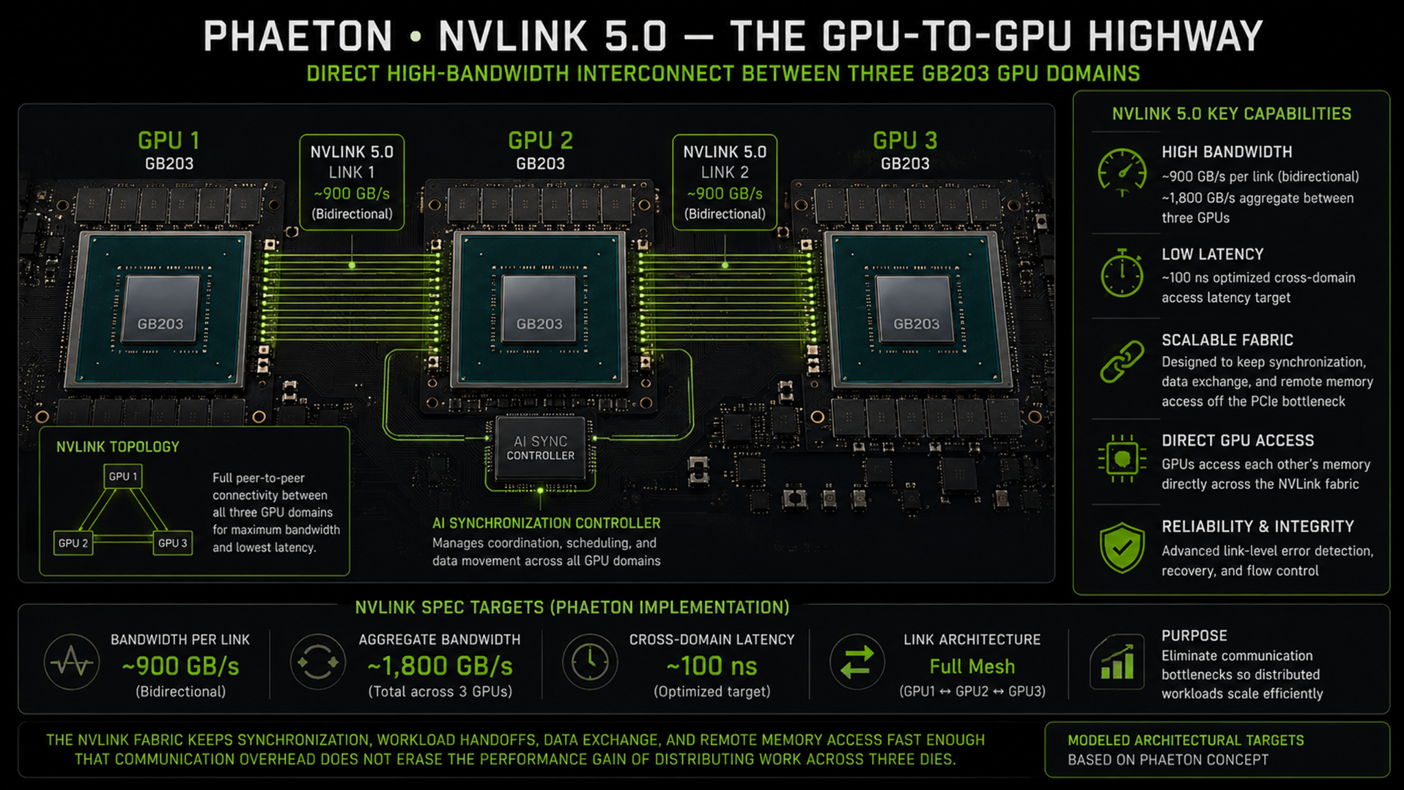
bidirectional
vs ~1,000 ns via PCIe
Shared Across 3 GPU Domains
Long dimension (~35 mm): Primarily driven by the edge-to-edge spacing between adjacent GPU footprints on the PCB. The high-speed routes must span that physical gap while remaining as short and uniform as the board architecture allows. Additional route length increases signal loss, skew, crosstalk exposure, and timing-margin pressure at very high signaling rates.
Short dimension (~13 mm): Driven primarily by routing density. Under PHAETON's preliminary routing model, 200 signal traces distributed across four PCB layers requires approximately 50 traces per layer. At an assumed 0.2 mm routing pitch, the signal field occupies roughly 10 mm before guard spacing and edge clearance are added, producing a total width of approximately 13 mm.
The result is a routing region with an approximate 3:1 rectangular proportion. Its geometry is driven primarily by die spacing, signal count, layer allocation, and signal-integrity requirements — not visual preference.
Each high-speed differential channel uses two closely matched traces. D+ and D− carry opposite-polarity versions of the signal, and the receiver measures the voltage difference between them. Electrical noise that couples similarly onto both traces appears as common-mode interference and is largely rejected by the receiver.
Net result: clean high-speed signaling across a short ~35 mm PCB route. Under PHAETON's preliminary routing model, the proposed inter-GPU region uses 200 high-speed signal traces distributed across multiple dedicated PCB layers. Additional reference-plane and ground structures provide the return paths and signal-integrity control required by the final implementation.
The exact lane count, signaling rate, ground-reference structure, and conductor allocation would depend on the final NVIDIA interconnect interface and PCB stackup. The purpose of the routing study is to demonstrate that a dense, short-reach, board-level interconnect region can be physically incorporated between the three GPU domains.
At 120 fps, each frame has approximately 8.3 ms to complete. A single ~100 ns cross-domain access consumes only a tiny fraction of that budget. The real challenge is repetition: remote accesses, synchronization barriers, workload handoffs, and dependent transfers can accumulate rapidly when they occur thousands or millions of times across a frame.
That is why latency matters as much as bandwidth. A low-latency direct interconnect is one of the major capabilities traditional consumer SLI lacked. PHAETON combines that fabric with hardware-assisted timing and coordination so domain-partitioned rendering has a better chance of remaining synchronized than two separate graphics cards communicating through a conventional PCIe-based multi-GPU path.
3x RTX 5080-class GB203 dies — 14″ unified PCB
GB203 × 3 · 48 GB GDDR7 total · 8 memory devices per GPU domain · NVLink 5.0 inter-GPU fabric · AI Synchronization Controller · 2× 16-pin power inputs · ~300 W target per die · adaptive domain-partitioned rendering
Explore the modeled PHAETON PCB architecture by selecting individual component groups. Each selection isolates a major board region and provides a short explanation of its proposed function within the platform.
GPU DOMAIN 1 — GB203
84 SMs
16 GB GDDR7 · 8 memory devices
256-bit · 960 GB/s local bandwidth
~300 W target
~54 TFLOPS modeled FP32 at 300 W
Primary domain: Geometry + rasterization
GPU DOMAIN 2 — GB203
84 SMs
16 GB GDDR7 · 8 memory devices
256-bit · 960 GB/s local bandwidth
~300 W target
~54 TFLOPS modeled FP32 at 300 W
Primary domain: Shading + lighting
GPU DOMAIN 3 — GB203
84 SMs
16 GB GDDR7 · 8 memory devices
256-bit · 960 GB/s local bandwidth
~300 W target
~54 TFLOPS modeled FP32 at 300 W
Primary domain: Ray tracing + compute
across 3 GPU domains
memory bandwidth
900 W GPU-domain allocation
Each GPU domain retains its own 16 GB local memory interface and 960 GB/s of local memory bandwidth. The proposed unified 48 GB memory model depends on software deciding when data remains local, when it is replicated, and when cross-domain access or transfer is worth its cost. The architecture is designed to maximize local memory use and reserve remote access for cases where duplication or transfer would be more expensive.
The production objective is for the driver and runtime to present PHAETON as one coordinated graphics platform while managing three internal GPU domains, their memory locality, power states, synchronization behavior, and workload distribution behind a unified software-facing device model.
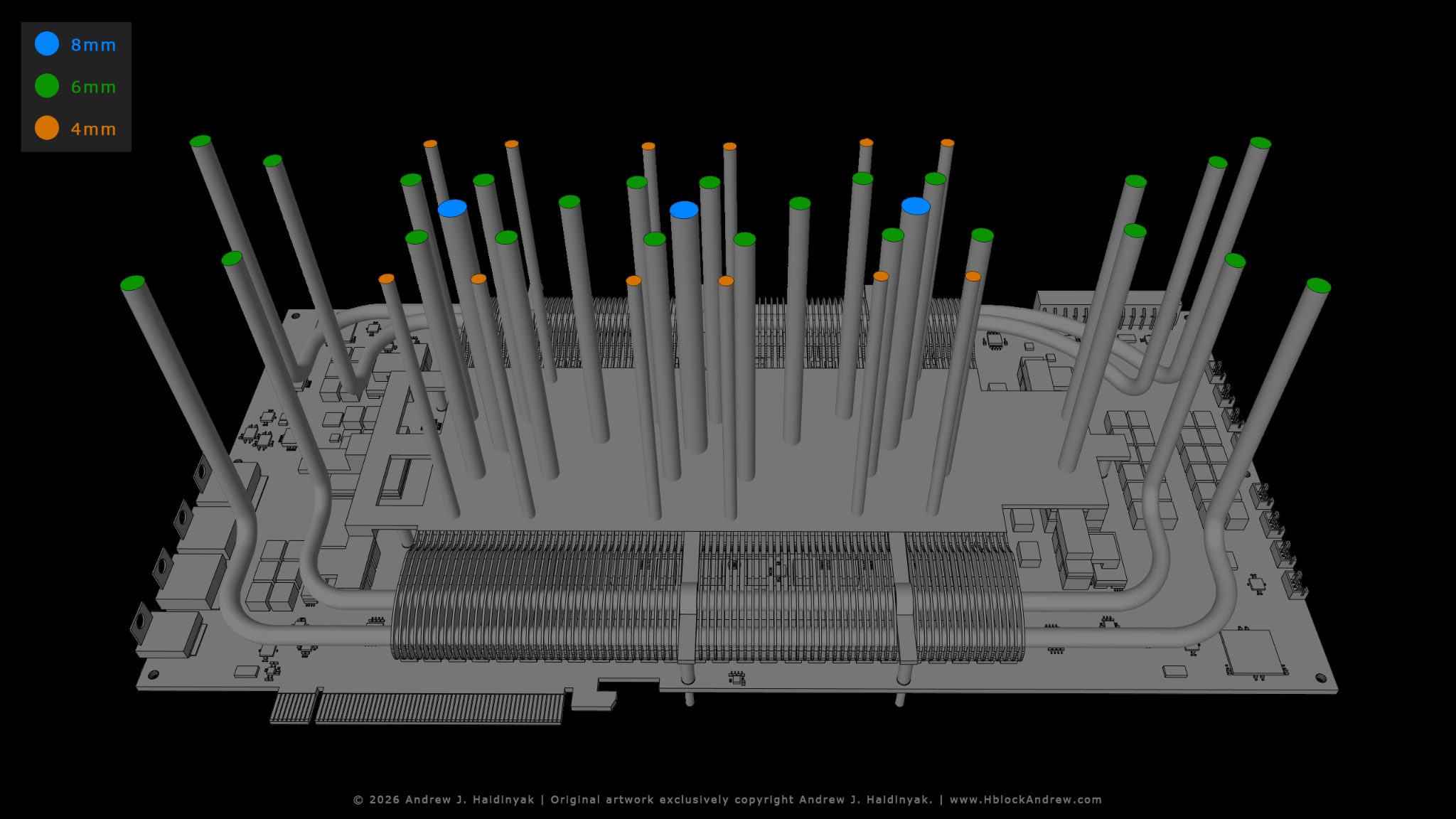
39 heat pipes. Zero compromises.
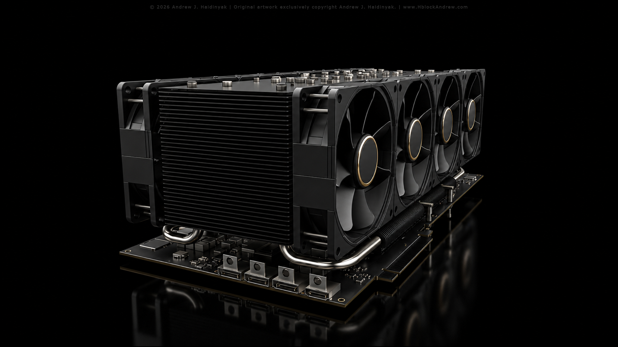
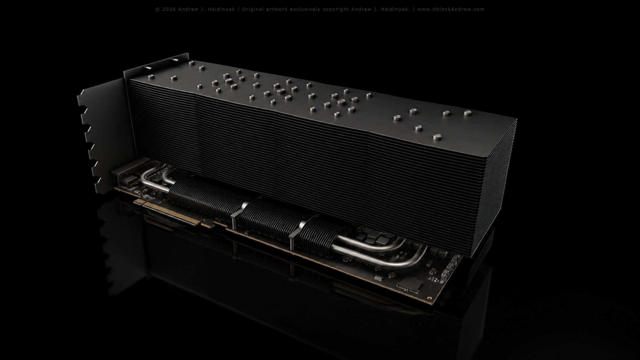
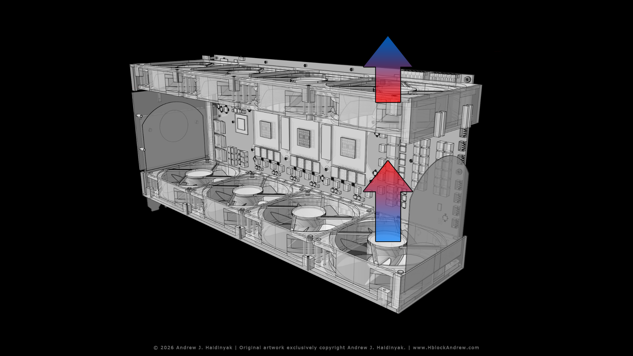
PHAETON is designed to turn physical size into a performance advantage. Its thermal architecture uses three distributed GPU heat sources, a large vapor chamber, thirty-nine heat pipes, an oversized fin field, and eight 92 mm fans to pursue a cooling class beyond conventional consumer graphics cards.
The objective is not simply to prevent throttling. PHAETON is explicitly designed to operate at lower sustained temperatures than air-cooled GPUs delivering comparable performance. By distributing approximately 900 W of GPU-domain power across three physical heat sources instead of concentrating comparable output into one dense package, the architecture creates more surface area for heat collection, more paths for heat transport, and more opportunity to remove that heat at lower airflow velocity.
The philosophy is closer to a high-performance workstation or server than a conventional gaming card: oversized thermal capacity, sustained-load stability, low thermal stress, and continuous performance over long operating periods. PHAETON is the consumer hot rod and the small developer's workhorse — a machine designed not only to reach high performance, but to keep delivering it.
PHAETON deliberately oversizes its thermal transport system relative to the nominal 900 W GPU-domain allocation. The objective is not to claim that every heat pipe carries an equal fraction of the load, but to create multiple parallel heat-transfer paths from the three GPU regions, memory zones, and vapor chamber into a large shared fin field.
That additional transport area is intended to reduce local thermal bottlenecks and lower the airflow required to maintain stable temperatures during sustained operation. In the PHAETON architecture, quiet operation is not treated as a separate feature; it is the intended consequence of distributed heat sources, oversized thermal transport, large fin area, and low-speed airflow.
The same thermal architecture is also intended to provide development headroom above the nominal operating target. A production team could evaluate higher board-power modes within the proposed 1,200 W power-delivery and thermal ceiling, but such operation would require validation of connector loading, VRM capacity, transient response, capacitor selection, PCB current density, vapor-chamber performance, heat-pipe transport limits, fin-stack rejection capacity, and chassis airflow.
The purpose of the 1,200 W ceiling is therefore not to promise a guaranteed overclocking mode. It is to avoid designing the cooling and structural systems directly against the nominal operating limit. Distribute the heat. Move it quickly. Reject it quietly.
The Efficiency Knee — Why PHAETON Targets 300 W per Die
GPU performance does not scale linearly with power. As voltage and frequency rise, additional wattage produces progressively smaller performance gains while heat density, electrical stress, and cooling demand continue to increase.
PHAETON is built around the opposite strategy: operate three GB203-class dies closer to the region where performance per watt remains strong, then combine their physical compute capacity across the platform. The architecture therefore targets approximately 300 W per GPU domain as a balance between sustained performance, thermal density, power-delivery load, and total board efficiency.
This is the mathematical core of PHAETON: distribute compute across multiple efficiently operated dies rather than forcing one larger die deeper into the diminishing-return region of its power curve.
theoretical stock FP32 baseline
600 W total GPU-domain power
Across three dies, that produces approximately 162 TFLOPS of aggregate physical FP32 throughput at 900 W of total GPU-domain power. At 200 W per die, the model projects approximately 47 TFLOPS per GPU domain, or roughly 141 TFLOPS of aggregate physical throughput at 600 W of total GPU-domain power.
The architectural advantage comes from using multiple dies closer to the stronger region of their performance-per-watt curve rather than extracting the final few TFLOPS from each die through progressively higher power. Real application performance would still depend on coordination overhead, workload scaling, memory locality, interconnect behavior, and software support.
A 900 W GPU changes the whole system
PHAETON targets approximately 900 W of total GPU-board power from the PSU. The power supply must therefore be sized for the complete computer rather than the graphics card alone. CPU demand, motherboard and VRM losses, memory, storage, cooling, USB devices, and transient headroom all sit above the GPU load.
The practical result is straightforward: 1,500 W is the entry point for a balanced PHAETON system, 1,600 W is the preferred class for most builds, and the heaviest workstation-style configurations move into the 1,800 W class.
from the PSU
PSU class
PSU class
20% sizing reference: ~1,409 W
Recommended PSU: 1,500 W minimum · 1,600 W preferred
20% sizing reference: ~1,362 W
Recommended PSU: 1,500 W minimum · 1,600 W preferred
20% sizing reference: ~1,590 W
Recommended PSU: 1,600 W minimum · 1,800 W preferred
20% sizing reference: ~1,530 W
Recommended PSU: 1,600 W minimum · 1,800 W preferred
| Platform load | Mid-range build | High-end build |
|---|---|---|
| Motherboard + board-level conversion losses | 45 W | 65 W |
| DDR5 memory | 15 W | 25 W |
| NVMe / SATA storage | 15 W | 30 W |
| CPU cooling + case airflow | 20 W | 30 W |
| USB devices + auxiliary headroom | 20 W | 25 W |
| Total modeled non-CPU / non-GPU allowance | 115 W | 175 W |
Phaeton is modeled to outpace the RTX 5090 by roughly 20–30% at 4K Ultra settings
PHAETON's revised performance model begins with approximately 162 TFLOPS of aggregate physical FP32 throughput at the 3×300 W GPU-domain target. After a modeled 10–15% coordination-overhead range, the architecture retains approximately 138–146 TFLOPS of modeled effective FP32-equivalent throughput, compared with roughly 105 TFLOPS for the RTX 5090 reference.
The memory argument is equally important: the three GB203 domains retain 2.88 TB/s of aggregate physical local memory-interface bandwidth. That figure is not one universally available shared pool, but it gives the architecture substantially more total local bandwidth than a single RTX 5090 while the NVLink fabric and software stack manage cross-domain movement, locality, and synchronization.
| Resolution | RTX 5090 avg FPS | PHAETON modeled avg FPS | PHAETON DLSS 4 model | Delta native |
|---|---|---|---|---|
| 1080p — ultra | 312 | 337 | 600+ | +8.0% |
| 1440p — ultra | 214 | 246 | 438 | +15.0% |
| 4K — ultra no RT | 138 | 173 | 309 | +25.4% |
| 4K — full path tracing | 62 | 82 | 148 | +32.3% |
| 8K — DLSS 4 + frame gen | 44 | 59 | 59 | +34.1% |
PHAETON only has a path to production because the wafer economics work. If this concept ever reaches the right hands, the architecture would still have to be seen as a worthy addition to NVIDIA's product lineup by the people responsible for deciding what gets built. Ultimately, that means convincing leadership at the highest level—including Jensen Huang—that PHAETON is not simply impressive, but valuable enough to manufacture, support, and sell.
The wafer-production analysis that follows is a strong indication that a Strike Cruiser-class GPU could become a profitable product. A reasonable real-world estimate for lifetime RTX 5090-class sales would be roughly 1.5 to 3 million units worldwide. PHAETON would enter a broader and potentially more exciting market position: above the conventional flagship, but far below the roughly $10,000 professional-class pricing of products such as the RTX PRO 6000 Blackwell.
That price gap matters. Many serious enthusiasts, creators, developers, small studios, and companies may consider spending roughly $2,000 to $3,000 on an entirely new class of high-performance GPU. Far fewer will spend around $10,000 for a professional card. PHAETON would target the people caught between those two markets—the users who want dramatically more capability than a conventional flagship but cannot justify enterprise-level pricing.
If the architecture performs as intended, the market opportunity could grow beyond the traditional RTX 5090-class audience. The excitement of the first Strike Cruiser-class GPU, combined with higher performance, greater memory capacity, a new multi-die architecture, and a price far below professional hardware, could expand demand rather than merely divide the existing flagship market.
This would be the first product of its kind. If it works, it will sell. And if it delivers what the following sections indicate is possible, I believe it could ultimately sell more units than any single RTX 5090-class flagship generation before it.
Production scale — die size, yield pressure, and manufacturing resilience
PHAETON's wafer-economics argument is not that three smaller dies are automatically cheaper than one large die. The more important question is how die size changes production behavior at scale. A smaller die creates more complete die opportunities per wafer and exposes less silicon area to any single random defect. PHAETON then uses three of those smaller dies per product. The result is a production tradeoff that changes as defect pressure rises.
Under the baseline model used here, one 300mm wafer produces approximately 70 gross GB202 die positions, compared with approximately 153 GB203 positions and 228 GB205 positions. After applying the same defect-density assumption to all three dies, the modeled defect-free output becomes approximately 33 GB202 dies, 105 GB203 dies, and 175 GB205 dies per wafer.
PHAETON does not therefore require three times as many wafers simply because it uses three GPU dies. Approximately 105 modeled defect-free GB203 dies can form about 35 complete three-die PHAETON sets, compared with approximately 33 defect-free GB202 dies available for single-die flagship products. The production value lies in how much finished-product output can be recovered from the same wafer resource—and how that relationship changes when defect pressure rises.
Gross whole-die positions are estimated with a standard edge-loss-adjusted 300mm wafer approximation. Modeled defect-free yield uses the same simplified Poisson relationship for every die. “Modeled defect-free dies” should not be read as marketable production yield: real semiconductor manufacturing also includes defect clustering, critical-area effects, parametric failures, harvesting, binning, packaging loss, and other factors not modeled here.
| Baseline production model | GB202 · RTX 5090 | GB203 · RTX 5080 | GB205 · RTX 5070 |
|---|---|---|---|
| Official die area | 750mm² | 378mm² | 263mm² |
| Approx. gross whole-die positions / wafer | ~70 | ~153 | ~228 |
| Modeled defect-free yield · D₀ 0.10/cm² | 47.2% | 68.5% | 76.9% |
| Modeled defect-free dies / wafer | ~33 | ~105 | ~175 |
| Finished product output from one wafer | ~33 single-die products | ~35 complete 3-die PHAETON sets | Reference only |
The modeled die counts in this section estimate completely defect-free silicon under a simplified Poisson defect model. Real GPU manufacturing is more flexible. Modern GPUs are designed with product configurations that allow portions of the full silicon layout to remain disabled while the remaining functional resources are validated for sale.
The full GB202 configuration contains 24,576 CUDA cores. The GeForce RTX 5090 activates 21,760—approximately 88.5% of the full configuration—while the RTX PRO 6000 Blackwell activates 24,064, or approximately 97.9%. This creates meaningful harvesting and binning flexibility: a die does not necessarily need every physical compute resource enabled to become a commercially useful product.
The same principle applies to GB203. The RTX 5080 uses the full 10,752-core configuration, while the RTX 5070 Ti uses a reduced 8,960-core configuration. A GB203 die that does not qualify for the full configuration may therefore retain value elsewhere in the product stack.
For this reason, the modeled defect-free counts shown in this section should not be interpreted as NVIDIA's actual commercial wafer yield. Real marketable output may be higher for both architectures after harvesting and binning. Because NVIDIA does not publish the required defect maps, qualification criteria, or product-bin distribution, this analysis keeps the comparison deliberately conservative and applies the same defect-free methodology to both dies.
This is a wafer-level silicon comparison only. It does not include die packaging, testing, binning, interconnect hardware, synchronization hardware, PCB complexity, cooling hardware, software development, validation, or complete product cost.
| Defect-density scenario | GB202 complete products / wafer | PHAETON complete 3×GB203 sets / wafer | Production result |
|---|---|---|---|
| D₀ = 0.03/cm² · low-defect case | ~56 | ~46 | GB202 advantage |
| D₀ = 0.05/cm² · strong-yield case | ~48 | ~42 | GB202 slight advantage |
| D₀ = 0.10/cm² · baseline model | ~33 | ~35 | Near parity · PHAETON slight advantage |
| D₀ = 0.20/cm² · high-defect stress case | ~16 | ~24 | PHAETON advantage |
The strategic value is therefore larger than a single per-die cost comparison. A multi-die platform built from an existing smaller die can reduce exposure to large-die yield pressure, require less recovery capacity after a poor wafer batch, and give production planners more flexibility in how silicon is allocated across the product stack. Whether those advantages outweigh the additional cost of multi-die packaging, synchronization hardware, software development, validation, and board complexity would require a full production program analysis.
From production resilience to field resilience
Section 13 examined what happens before a GPU leaves the factory: wafer geometry, defect density, harvesting, and production yield. Section 14 asks the next question: what happens after the product enters the real world?
A high-performance graphics platform must survive years of thermal cycling, sustained electrical load, shipping shock, installation stress, case-airflow variation, cable handling, and system-side power variability. Public failure-rate data for individual NVIDIA GPU dies is not available, so this section does not assign unsupported field-failure percentages to GB202 or GB203. Instead, it compares where stress is concentrated, what a critical failure means to the complete product, and which architectural features may improve resilience.
| Reliability condition | Single-die flagship architecture | PHAETON design objective |
|---|---|---|
| Primary GPU-domain failure | Complete graphics-card outage | Potential isolated-domain service mode |
| Physical compute remaining after one domain loss | 0% | Up to ~67% theoretical physical capacity before system effects |
| Recovery behavior | Repair or replacement required | Reduced-service target pending firmware, driver, memory, and interconnect validation |
| Failure concentration | One critical compute package | Three independent compute domains with potential fault isolation |
| Thermal factor | Single flagship architecture | PHAETON concept |
|---|---|---|
| Primary heat-source concentration | One large, dense thermal source | Three distributed thermal sources |
| Per-domain operating strategy | One flagship die carries the full graphics workload | ~300W target per GB203 domain near the modeled efficiency knee |
| Thermal transport system | Reference and AIB cooler dependent | Oversized vapor chamber, 39 heat pipes, large fin field, 8× 92mm fans |
| Reliability interpretation | Thermal and mechanical stress concentrated around one primary package | Lower modeled per-domain temperatures and smaller thermal swings may reduce cycling severity |
| Stress mechanism | RTX 5090-class reference point | PHAETON design objective |
|---|---|---|
| Primary input architecture | Up to 575W through one 600W-class 16-pin input | ~900W target divided across two 600W-class 16-pin inputs |
| Nominal connector loading | ~95.8% of one connector's nominal maximum | ~75% per connector under balanced 450W / 450W operation |
| Connector risk interpretation | Greater current concentration and less nominal operating margin | Lower current concentration per input and more nominal headroom |
| Cooler and card load path | PCB, bracket, motherboard slot, and user-added support dependent | Rigid frame, 13 PCB-to-backplate mounts, 8 central support locations, and chassis support |
| Long-term mechanical objective | Large cantilever load can increase board and slot stress | Transfer more static mass away from the PCB and PCIe slot |
Three physical heat sources spread thermal load across a much larger area. The value is not a guaranteed temperature result; it is reduced heat-flux concentration and more surface area available for thermal transport.
Two primary power inputs reduce the amount of current concentrated through any one connector. Greater nominal headroom is intended to improve tolerance for real-world cable, seating, and sustained-load variation.
A three-domain architecture creates a path toward fault isolation that a single critical compute package cannot provide. The engineering challenge is making the rest of the platform capable of using that redundancy.
Public failure-rate data for individual NVIDIA GPU dies is not available, so this section does not claim a validated field-failure percentage for GB202 or GB203. Instead, it compares the architectural stress mechanisms and failure consequences created by each design. By deliberately allowing PHAETON to be physically larger, the architecture can prioritize standard-sized, readily available components and more generous spacing instead of forcing equivalent capability into smaller, more specialized parts that may require additional engineering, packaging, and manufacturing expense.
PHAETON's reliability argument is based on distributed heat sources, lower modeled per-domain operating temperatures, greater connector headroom, reinforced mechanical support, and the possibility of isolating a failed GPU domain. These features may reduce specific forms of thermal, electrical, and mechanical stress, but their real effect on product failure rate would require prototype testing, accelerated life testing, vibration and drop validation, connector thermal testing, and long-term field data.
The objective is not to claim fault immunity. It is to design for lower stress concentration and greater operational resilience.
What changes when manufacturing conditions change?
Section 13 established the wafer model. Section 14 examined field reliability after shipment. This section now stress-tests the production strategy itself: where the monolithic GB202 architecture is more efficient, where the three-GB203 architecture crosses into an advantage, and how each responds when part of a production run suffers a yield excursion.
| Metric | 1× GB202 flagship | 3× GB203 PHAETON | Production delta |
|---|---|---|---|
| Modeled defect-free yield | 68.7% | 82.8% per GB203 die | — |
| Wafers required for 1M products | ~20,786 | ~23,687 | PHAETON requires ~2,901 more wafers |
| Interpretation | When defect density is low, the single large die converts wafer capacity into finished products more efficiently because PHAETON must supply three qualified dies per board. | ||
| Metric | 1× GB202 flagship | 3× GB203 PHAETON | Production delta |
|---|---|---|---|
| Modeled defect-free dies per wafer | ~33.1 | ~104.8 GB203 dies | — |
| Wafers required for 1M products | ~30,243 | ~28,615 | PHAETON requires ~1,628 fewer wafers |
| Modeled raw wafer input | ~$544 per product | ~$515 per product | ~$29 lower per product · ~5.4% |
| One-million-product scale | Assuming $18,000 per wafer | ~$29.3M lower modeled raw wafer input | |
| Metric | 1× GB202 flagship | 3× GB203 PHAETON | Recovery delta |
|---|---|---|---|
| Additional recovery wafers | ~1,685 | ~930 | ~755 fewer recovery wafers |
| Modeled recovery wafer burden | ~$30.3M | ~$16.7M | ~$13.6M lower |
| Operational consequence | The smaller-die architecture needs less replacement wafer capacity to restore the same one-million-product target after an underperforming portion of the production run. | ||
Under the baseline model used in this document, one million PHAETON products require approximately 1,628 fewer wafers than one million GB202-based products, representing approximately $29.3 million less modeled raw wafer input under the stated $18,000 wafer-cost assumption.
The largest strategic difference appears when production conditions deteriorate. In the modeled 10% yield-excursion scenario, GB202 production requires approximately 1,685 additional recovery wafers, compared with approximately 930 for the three-GB203 architecture. The PHAETON production strategy therefore requires roughly 755 fewer recovery wafers to restore the same one-million-product target.
The value of the multi-die architecture is not that smaller dies always win. Its production value lies in becoming progressively less exposed to large-die yield pressure as manufacturing conditions worsen.
What could the product line be worth at market scale?
The previous sections examined whether PHAETON can make sense as an architecture and as a production strategy. This section asks a simpler business question: if the complete GeForce lineup follows the broad sales pattern established by the RTX 40-series generation, where could a new Strike Cruiser-class product fit—and what direct product value could it create?
across seven products
scenario target
contribution per unit
direct contribution
| Product | Modeled lifetime units | Reference MSRP | Modeled direct product burden | Modeled direct contribution / unit | Modeled lifetime direct contribution |
|---|---|---|---|---|---|
| RTX 5060 | 14.0M | $299 | $178 | $121 · 40.5% | ~$1.69B |
| RTX 5060 Ti | 9.0M | ~$404 blended | $225 | $179 · 44.3% | ~$1.61B |
| RTX 5070 | 7.0M | $549 | $286 | $263 · 47.9% | ~$1.84B |
| RTX 5070 Ti | 5.0M | $749 | $363 | $386 · 51.5% | ~$1.93B |
| RTX 5080 | 2.3M | $999 | $455 | $544 · 54.5% | ~$1.25B |
| RTX 5090 | 1.3M | $1,999 | $910 | $1,089 · 54.5% | ~$1.42B |
| PHAETON | 2.8M | $2,714 | $1,425 | $1,289 · 47.5% | ~$3.61B |
The 5060- and 5070-class products are modeled as the volume engines because mainstream price tiers historically reach far more buyers than enthusiast flagships. The high-end cards sell fewer units but create substantially more direct contribution per sale.
PHAETON is modeled above RTX 5090 volume because it would not compete only for the existing flagship gamer. Its 48GB memory target, multi-die compute, creator and AI potential, and price far below professional workstation hardware could pull demand from users who currently have no practical product between a $1,999 flagship and five-figure professional GPUs.
The modeled contribution figures subtract direct product burdens only: hardware, assembly, packaging, outbound logistics, and warranty reserve. They do not subtract research and development, software engineering, validation programs, corporate overhead, channel incentives, taxes, or other operating expenses.
If the architecture does not deliver its promised performance, software support, or reliability, this demand case does not hold.
PHAETON value engineering — where the money goes
PHAETON is not designed to be a cheaper RTX 5080. It is designed to use roughly three times the retail budget to assemble a much larger physical computing platform. The core value question is therefore not whether it costs more, but whether the additional cost creates proportionally greater capability. Under the current model, PHAETON targets approximately 2.4–3.0× the compute capability and 3× the VRAM capacity at approximately 2.72× the RTX 5080 reference MSRP.
$2,714 vs $999
171 vs 57 TFLOPS
138–146 vs 57 TFLOPS
48GB vs 16GB
$999 reference MSRP
~57 TFLOPS theoretical stock FP32
16GB GDDR7
1× GB203-class GPU die
The RTX 5080 remains the conventional high-end reference point: one die, one memory domain, and a much lower entry price.
$2,714 target MSRP
~171 TFLOPS theoretical stock aggregate
~138–146 TFLOPS modeled effective-equivalent
48GB total GDDR7 target
3× GB203-class GPU dies
PHAETON asks the buyer to pay roughly 2.72× more for a platform targeting up to 3× the installed theoretical compute and 3× the VRAM capacity.
PHAETON modeled factory BOM — high-volume production scenario
Estimated range: ~$1,280–1,445| Category | Modeled cost | Basis | Interpretation |
|---|---|---|---|
| AI synchronization controller | ~$25–40 | Dedicated controller / repurposed high-volume silicon scenario | Final implementation could materially change cost |
| 48GB GDDR7 | ~$300–350 | 24 × 2GB devices · modeled high-volume pricing | One of the largest BOM uncertainties |
| Board, power and I/O | |||
| PCB + VRM + I/O | ~$220–250 | 10-layer high-current board · 54 total VRM phases · dual 16-pin input · controllers and passives | Large physical board reduces some miniaturization pressure but remains electrically complex |
| Thermal and mechanical platform | |||
| Thermal solution | ~$135–165 | Vapor chamber · 39 heat pipes · fin stack · 8× 92mm fans · TIM · shroud | Large and visually dominant, but not the primary cost driver |
| Mechanical structure | ~$15–25 | Rigid backplate/frame · mounting hardware · chassis support system | Physical size is used as an engineering resource rather than minimized at any cost |
| Manufacturing completion | |||
| Assembly, test, burn-in and retail packaging | ~$70–100 | Three-die validation · extended functional test · retail packaging | Higher than a conventional single-die card because coordination must be validated |
hardware + assembly + test
adds logistics + warranty reserve
at $2,714 MSRP
vs RTX 5080
| Value metric | RTX 5080 | PHAETON | PHAETON value position |
|---|---|---|---|
| Reference / target MSRP | $999 | $2,714 | 2.72× the purchase price |
| Theoretical stock aggregate FP32 | ~57 TFLOPS | ~171 TFLOPS | 3.0× installed theoretical compute |
| Modeled effective-equivalent FP32 | ~57 TFLOPS | ~138–146 TFLOPS | ~2.4–2.6× after modeled coordination loss |
| Installed VRAM capacity | 16GB | 48GB | 3× capacity |
| Theoretical FP32 per dollar | ~0.057 TFLOPS/$ | ~0.063 TFLOPS/$ | ~10% higher |
| Modeled effective-equivalent FP32 per dollar | ~0.057 TFLOPS/$ | ~0.051–0.054 TFLOPS/$ | ~6–11% lower after modeled overhead |
| Purchase price per GB of installed VRAM | ~$62.44/GB | ~$56.54/GB | ~9% lower |
A simple way to understand PHAETON's consumer value is to compare it with buying three RTX 5080 cards separately.
At the RTX 5080 reference price of $999, three cards cost $2,997 before tax. Using an example 10% sales-tax rate, the buyer pays approximately $299.70 in tax, bringing the total purchase cost to $3,296.70.
One PHAETON at the $2,714 target MSRP would generate approximately $271.40 in sales tax under the same example rate, bringing the total purchase cost to $2,985.40.
The consumer therefore pays approximately $311.30 less at checkout for one PHAETON than for three separate RTX 5080 cards. That includes $283 less in product cost and approximately $28.30 less in sales tax.
For the buyer, the comparison is simple: one coordinated three-die platform, one purchase, one board, and a lower total checkout cost than buying three RTX 5080 cards separately.
Example uses a 10% sales-tax rate. Actual taxes vary by location.
These price estimates are based on current market values and the production-cost assumptions used throughout this document. Future component costs may be lower as manufacturing capacity for GDDR7 memory, power-delivery components, cooling hardware, and other high-volume parts expands to meet demand.
Greater production scale, improved yields, supplier competition, and more mature manufacturing processes could reduce the final cost of building PHAETON over time.
Potentially protectable innovations — candidate IP areas
PHAETON identifies several technical areas that may justify formal patentability review. The architecture has been independently documented since April 2026, but the existence, scope, ownership, and enforceability of any future patent rights would depend on professional prior-art searching, inventorship analysis, claim drafting, filing strategy, and patent examination.
As the creative architect of PHAETON, I do not intend to file patent claims against this concept for the purpose of blocking its development, extracting licensing fees, or holding future engineering progress hostage.
I would only consider participating in patent filings if I were formally hired by NVIDIA for work connected to PHAETON or its presentation, development, or marketing. In that situation, ownership of any patentable work would be governed by the terms of the employment or contract agreement. Any artwork, design material, or other work specifically excluded by that agreement would remain subject to the rights defined in the contract.
I will not become a patent troll, and I will not use intellectual property as a weapon for ego, obstruction, or petty control. Patent trolls exist. They hold up progress without building the future themselves. That is not what PHAETON was created to become.
The purpose of documenting these candidate invention areas is to preserve the engineering record, identify what may deserve legitimate protection if the architecture moves toward production, and help ensure that the engineering of the Phaeton is not impeded by lesser minds.
identified for review
documentation timeline
by this document
still required
| Candidate IP family | Potentially protectable subject matter | Why it matters | Current status |
|---|---|---|---|
| A · Multi-die coordination controller | |||
| Real-time hardware workload arbitration | Synchronization signaling, frame-completion prediction, workload balancing, deadline-aware redistribution, inter-die latency compensation, and final frame assembly. | The possible invention is not the broad idea of synchronizing multiple GPUs. The strongest opportunity would be a specific controller mechanism: what it measures, what decisions it makes, how work is reassigned, and how frame timing is stabilized. | Formal prior-art and patentability review required |
| B · Render-domain partitioning | |||
| Dynamic division of one workload across homogeneous dies | Variable render-domain sizing, locality-aware assignment, deadline-based rebalancing, transfer minimization, and power-state-aware scheduling. | PHAETON's value may lie in the specific rules used to divide, resize, transfer, and recombine work across multiple physical GPU domains rather than in multi-GPU rendering as a broad concept. | Formal prior-art and patentability review required |
| C · Power-aware multi-die operation | |||
| Efficiency-targeted workload distribution | Redistributing work among multiple dies according to power limits, thermal headroom, efficiency targets, and changing workload intensity. | A coordinated system that intentionally moves work to keep several dies near a desired operating region may offer a protectable implementation if the control logic is specific and distinguishable from prior systems. | Formal prior-art and patentability review required |
| D · Memory coordination architecture | |||
| Locality-aware multi-die memory management | Software-visible memory behavior, replication versus remote access decisions, ownership policies, migration rules, resource placement, and transfer prioritization. | The candidate invention would need to be the specific memory-management mechanism. Broad concepts such as unified memory, shared address spaces, or memory pooling should not be treated as automatically novel. | Formal prior-art and patentability review required |
| E · Thermal and mechanical architecture | |||
| Integrated cooling and structural system | Multi-die vapor-chamber geometry, heat-pipe topology, airflow routing, fan-idle transition behavior, backplate support, mounting load paths, and serviceability. | The possible value is in the functional arrangement and interaction of the cooling and structural elements. Individual features such as multiple heat pipes, large heatsinks, or fan-idle modes should not be assumed to be independently protectable. | Formal prior-art and patentability review required |
Specific mechanisms matter more than broad ideas. Timing diagrams, control logic, decision thresholds, data paths, failure handling, hardware interfaces, and clearly defined operating sequences would make future claim analysis substantially stronger.
The April 2026 project record helps show what the concept contained and when it was documented. That record is technically useful, but it is not presented here as a substitute for a patent filing, an inventorship determination, or a professional legal opinion.
A serious IP review would map each candidate mechanism against existing patents and technical literature, identify the narrowest differentiating features, determine inventorship, and decide which concepts are worth drafting into formal claims.
48GB of local AI headroom — without buying data-center hardware
PHAETON is not presented as a replacement for a data-center accelerator. Its purpose is to fill the large price and capability gap between ordinary consumer GPUs and professional or data-center hardware by giving local users substantially more physical GPU memory and multi-die compute capacity in one platform.
32GB GDDR7
48GB total GDDR7
96GB ECC GDDR7
data-center accelerator
| GPU tier | Price reference | GPU memory | Memory bandwidth | Published / modeled AI capability | Primary role |
|---|---|---|---|---|---|
| RTX 5090 | $1,999 reference MSRP | 32GB GDDR7 | 1.792 TB/s | 3,352 AI TOPS | Consumer flagship · gaming · creator AI |
| PHAETON | $2,714 target MSRP | 48GB total physical GDDR7 | 3× 960 GB/s local interfaces 2.88 TB/s aggregate local bandwidth across three dies; not one shared memory bus |
5,403 AI TOPS theoretical stock aggregate 3× RTX 5080 resources before coordination and software overhead |
New local-AI / creator tier · multi-die consumer platform |
| RTX PRO 6000 Blackwell | $13,250 current NVIDIA marketplace listing | 96GB ECC GDDR7 | 1.792 TB/s | 4,000 AI TOPS | Professional workstation · certified enterprise workflows |
| NVIDIA H100 80GB | $25,000–40,000 current accelerator market range | 80GB HBM3 / HBM2e depending on form factor | Up to 3.35 TB/s | Data-center Tensor performance is precision- and form-factor-dependent; not directly comparable to Blackwell RTX AI TOPS | Data-center training · inference · scaled server deployment |
| Local AI workload class | RTX 5090 · 32GB | PHAETON · 48GB target | RTX PRO 6000 · 96GB | H100 · 80GB |
|---|---|---|---|---|
| Large-model local inference | ||||
| Large quantized LLMs | Strong, but tighter model/context headroom | More room for weights, context, KV cache, and runtime overhead | Very large local models and professional workflows | Data-center inference at enterprise scale |
| Multi-model and multimodal pipelines | Combined models can create memory pressure | Greater ability to keep several model stages resident locally | Large professional pipelines | High-throughput server pipelines |
| Generative media | ||||
| Image generation | Excellent consumer capability | Larger batches, multi-model workflows, and more working headroom | Professional-scale local workflows | Usually not the economic reason to buy H100 |
| Video generation | Capable; memory pressure rises quickly with workflow size | More room for frames, resolution, models, and pipeline stages | High-end professional local generation | High-throughput data-center generation |
| Development and creation | ||||
| Local AI development | Strong single-user platform | Designed for larger resident models and multi-die experimentation | Professional development with 96GB ECC memory | Enterprise deployment, training, and inference |
| Large 3D / reconstruction working sets | Strong, project-size dependent | More working-set headroom before memory pressure | Very large professional projects | Specialized compute rather than workstation graphics focus |
Local AI users often optimize around memory ceilings before they run out of raw compute. More physical GPU memory can reduce offload, increase context and batch headroom, support larger working sets, and keep more of a complex pipeline resident on the GPU platform.
The RTX PRO 6000 Blackwell shows what buyers can purchase when 32GB is not enough: 96GB of ECC GDDR7, professional drivers, certification, and workstation support. It also shows the price jump. PHAETON targets a lower tier for buyers who need more local capacity but do not need every professional feature.
H100 remains the data-center reference point because its memory system, Tensor performance, NVLink, deployment model, and enterprise ecosystem are built for server-scale AI. PHAETON's argument is not that those advantages disappear. It is that many independent developers, creators, researchers, and small studios do not need to buy that entire class of infrastructure.
Beyond raw VRAM — PHAETON, NTC, and the future of gaming hardware
PHAETON is not only a high-end graphics card concept. It demonstrates a broader gaming architecture: multiple coordinated GPU domains, substantial physical memory, and neural-compute resources working together. At full scale, that architecture can serve developers. Scaled downward, the same design philosophy could become a fixed gaming platform built to play the software created on it.
3× RTX 5080-class GPU domains · 48GB total physical GDDR7 target
Designed for game-engine development, high-end asset creation, neural rendering, NTC development and validation, local AI tools, large creator workloads, and the full-scale exploration of multi-domain rendering.
Conceptual 3× RTX 5070-class GPU domains · approximately 32GB total GDDR7
A lower-power derivative could preserve the same broad coordination model while reducing cost, power, cooling requirements, and total compute. The goal is not to copy three retail RTX 5070 cards. It is to scale the architecture into purpose-built fixed hardware.
| Platform role | Full PHAETON | Scaled PHAETON derivative |
|---|---|---|
| Primary purpose | Build, test, train, create, and validate | Play, stream, create, and run the finished software |
| Conceptual GPU class | 3× RTX 5080-class domains | 3× RTX 5070-class domains or future equivalent |
| Total physical memory target | 48GB GDDR7 | Approximately 32GB GDDR7 |
| Hardware philosophy | Maximum development headroom | Fixed, lower-power gaming target |
| Software role | Development workstation and reference architecture | Purpose-built Linux gaming OS with Steam integration |
| Shared direction | Multi-domain coordination · neural rendering · NTC · known workload-partitioning model | |
Neural Texture Compression should not be used as an excuse to build hardware with too little memory. The stronger approach is to begin with a substantial physical memory base, then use neural compression to make that memory go further.
A fixed platform gives engine teams a known number of compute domains, a known memory target, a known neural-rendering baseline, and a stable optimization target. That can be easier to design around than optional multi-GPU support across thousands of unrelated PC configurations.
A purpose-built Linux gaming OS with Steam integration could combine a fixed hardware target with a broader PC software ecosystem. The platform direction is more open than a traditional closed console while still giving developers hardware they can explicitly optimize for.
Built like it needs to last.
PHAETON is deliberately larger than a conventional graphics card because the architecture prioritizes cooling capacity, structural support, component spacing, serviceability, and controlled load paths over compactness. The card is treated as a mechanical system, not simply a PCB with a cooler attached.
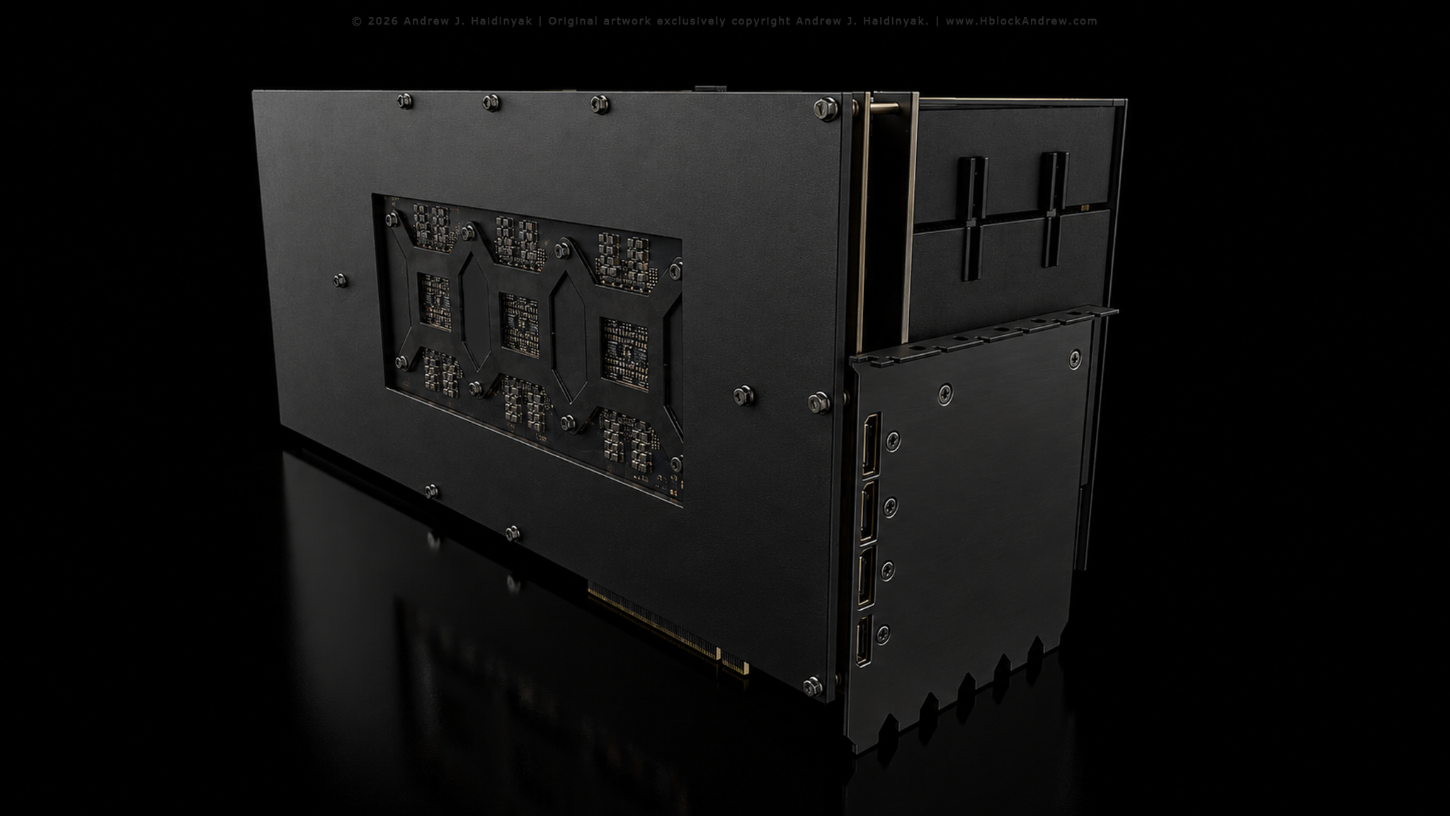
A purpose-built chassis uses a dedicated GPU rail, cradle, or floor-supported structure to carry the majority of card mass. The PCIe connector provides data and electrical interface; it is not expected to act as the primary structural support for a 7–10 lb assembly.
The PCB, vapor chamber, backplate, perimeter supports, package-clamping points, and frame are treated as separate mechanical elements with defined jobs. Card mass, cooler mass, and GPU contact pressure should not be allowed to become one uncontrolled bending load on the PCB.
The larger form factor creates room for replaceable fans, accessible fasteners, fin cleaning, thermal-assembly inspection, and easier PCB service. The design uses size to reduce packaging pressure and simplify maintenance instead of treating compactness as the highest priority.
| Mechanical element | PHAETON design role |
|---|---|
| Custom chassis support | Primary system-level support for the 7–10 lb card assembly; designed to transfer most static card mass into the case structure instead of the motherboard slot. |
| Backplate support points | Control PCB deflection, preserve designed clearances, distribute structural load, and stabilize the board across its full length. |
| GPU / vapor-chamber clamping points | Maintain controlled package contact pressure and distribute thermal-interface load without using the PCB as an uncontrolled spring. |
| Aluminum frame and backplate | Provide rigidity without the unnecessary mass penalty of an equivalent steel structure. |
| Transport restraint | Shipping and transport remain separate engineering conditions; the chassis must positively restrain the card against multi-directional shock rather than relying only on installed static support. |
8× 92mm fans · 4 push + 4 pull
362 × 97 × 39 mm fin field
38 aluminum fins · matte black anodized
8 mm multi-die vapor chamber
39 total heat pipes
Nickel-plated copper heat-pipe surfaces
700 RPM · idle and light load
900 RPM · quiet sustained target
1,200 RPM · heavy sustained load
1,700 RPM · high-thermal operating ceiling
Standard-sized fans are easier to inspect, clean, and replace than deeply integrated proprietary blower assemblies.
The oversized assembly creates room for service access to fasteners, structural supports, the fin field, and thermal components.
Cooling capacity and low-RPM operation are prioritized so the card does not need to behave like a compact product pushed to its acoustic and thermal limits.
Every number.
PHAETON's full specification sheet separates inherited reference data, direct three-die arithmetic, architectural targets, modeled estimates, and items that still require production validation.
Where concept architecture ends — and production engineering begins
PHAETON defines a board-level architecture, operating strategy, thermal philosophy, power target, structural system, and software direction. Moving from concept to product requires access to proprietary silicon behavior, power-management interfaces, interconnect capabilities, firmware controls, manufacturing limits, and test infrastructure that are not available from public information alone.
The validation framework below is provided as an educational reference outlining the testing, simulation, failure analysis, dependency review, and production decisions required to move from an architecture study toward real hardware. It is not a substitute for a manufacturer validation program and does not assume success. Its purpose is to identify what must be tested, what can fail, what depends on proprietary platform access, and what must be proven before production.
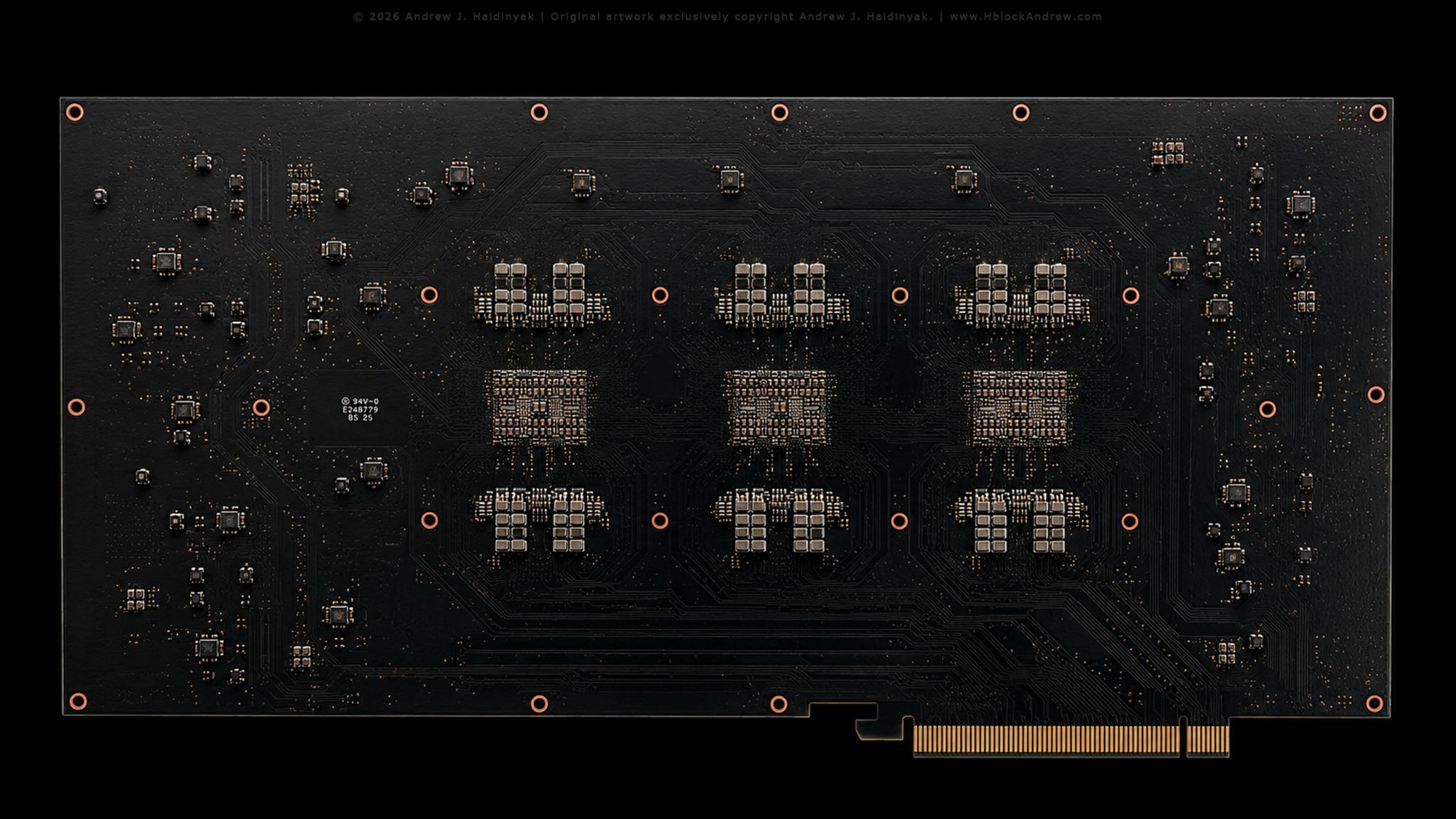
Validate plane current density, neck-down regions, connector entries, vias, layer transitions, VRM feed points, transient response, input sharing, and the behavior of all three GPU domains under independent and simultaneous load steps.
Prove that the physical link, protocol, bandwidth, latency, routing, signal integrity, fault behavior, and memory-coordination model are sufficient for the selected workload-partitioning strategy.
Measure real heat rejection, fan interaction, tonal noise, structural deflection, chassis load transfer, transport restraint, and the first component that reaches a limiting temperature under sustained operation.
Can the PCB distribute current without unacceptable local heating? What copper weight, via density, plane geometry, and redundant current paths are required at connector entries, neck-down regions, VRM feeds, and layer transitions?
What happens when one, two, or all three GPU domains change load at once? How does the platform prevent synchronized load steps from creating excessive voltage droop, overshoot, input-current spikes, or connector imbalance?
How are both 16-pin inputs balanced? What happens during partial insertion, rising connector temperature, sustained current imbalance, or loss of one input? Can the system enter a safe reduced-power service mode?
What silicon interface is actually available? What bandwidth and latency are required for each workload mode? How are traffic priorities, packet loss, degraded links, and recovery handled?
Do the differential-pair assumptions survive insertion loss, crosstalk, skew, return loss, vias, connector transitions, and manufacturing variation across the full board?
The architecture succeeds only if the inter-die communication system is fast enough, predictable enough, and fault-tolerant enough for the selected workload model.
Which resources remain local, which are replicated, when is remote access acceptable, and how much bandwidth is lost to migration, duplication, or cross-die traffic?
How does the driver expose the 48GB total physical memory target? What happens when one domain exhausts local memory? How are pathological transfer patterns detected and corrected?
Can the cooler reject the 900W nominal board target continuously? Which component becomes the first thermal limit: GPU package, memory, VRM, vapor chamber, heat pipes, fin stack, power connector, or chassis exhaust?
Do measured temperatures track the current design targets at 700, 900, 1,200, and 1,700 RPM? How do ambient temperature and chassis airflow shift the curve?
Do eight push-pull fans create tonal peaks, beat frequencies, motor resonance, shroud turbulence, or structure-borne vibration that are more intrusive than the overall dB(A) level suggests?
Do measured results approach the current 16 / 20 / 25 / 32 dB(A) targets at 700 / 900 / 1,200 / 1,700 RPM?
How much card mass is transferred into the chassis structure? How much residual load remains at the PCIe interface after the support system is engaged?
Do the PCB, backplate, vapor chamber, clamping points, and chassis support remain aligned during repeated heating and cooling cycles?
What restraint is required for shipping and system transport? Static chassis support and dynamic shock protection must be engineered as separate problems.
How does the system react to connector overtemperature, fan failure, pump-free cooler degradation, sensor faults, link faults, memory errors, or one unavailable GPU domain?
Can the platform deliberately transition between single-die, two-die, and three-die operation according to software support, power availability, thermal state, or component faults?
Does one GB203-class domain behave like a conventional rendering device for unsupported applications? Are display ownership, memory mapping, firmware, and driver exposure stable?
Which engines and workload classes scale well? Which do not? How are frame pacing, latency, workload imbalance, and fallback behavior measured?
Can workloads move between operating modes without restart, corruption, or unacceptable latency? How quickly can the system fall back when scaling is unsupported?
Can the PCB, vapor chamber, 39-pipe thermal assembly, eight fans, support frame, and custom chassis interface be built repeatedly within acceptable tolerances?
What test points, telemetry hooks, automated checks, and burn-in procedures are required before shipment?
Can fans, shrouds, support hardware, and thermal components be inspected or replaced without creating unnecessary PCB damage or complete product disposal?
How does the system behave under sustained full load, elevated ambient temperature, dust loading, degraded fan operation, repeated power cycling, and long-duration mixed workloads?
Can the system survive one-domain faults, one-input faults, sensor faults, or partial cooling degradation without creating unsafe conditions or unnecessary total loss of the product?
PHAETON should advance through a staged validation process so that the most expensive and difficult failures are discovered as early as possible, before additional time and resources are committed to later development stages.
Power integrity, signal integrity, current density, stackup, connector behavior, and VRM transients before fabrication.
Dummy heat loads, vapor chamber, fin stack, airflow, acoustic behavior, support structure, and chassis integration before live GPU silicon.
Bring up one GPU domain first, then two, then all three. Validate power, telemetry, memory, links, and thermal response incrementally.
Single-die compatibility, two-die scaling, full three-die coordination, mode switching, workload partitioning, frame pacing, and fault recovery.
Manufacturing yield, endurance, safety, acoustics, service procedures, packaging, transport, and repeatable end-of-line testing.
No modeled claim becomes a product specification until the relevant stage produces measured evidence that the design meets the target.
A new platform class creates new directions
PHAETON is not only an attempt to create a faster graphics card. It is an attempt to open a new design space for NVIDIA: a scalable multi-domain platform architecture that could support multiple products instead of ending as one experimental flagship.
My name is Andrew J. Haidinyak. I am presenting PHAETON: HB3×RTX 5080 not simply as a proposal for a faster graphics card, but as a proposal for a new class of NVIDIA platform.
The concept combines three coordinated GPU domains, large local memory capacity, distributed power delivery, dedicated coordination hardware, oversized air cooling, and a rigid chassis-supported structure into one board-level architecture. The point is not that every future NVIDIA GPU should resemble PHAETON. The point is that a new platform class creates options.
NVIDIA is already king of the hill. That is exactly why it is positioned to evaluate what comes next rather than simply defend the current product ladder.
I am not asking NVIDIA to accept every implementation detail exactly as drawn. I am asking NVIDIA to determine whether the architecture contains enough technical and commercial potential to justify deeper investigation. The three questions below are the decision framework.
CONCEPT DESIGN · APRIL 2026
PHAETON · HB3×RTX 5080
——————————————————
Can three coordinated GPU domains operate as one practical consumer platform with acceptable interconnect, scheduling, memory, latency, power, and software overhead?
Can the architecture support enough useful products and workloads to justify the engineering investment required to develop it?
Which mechanisms—interconnect, synchronization, memory policy, power delivery, cooling, structure, or software orchestration—should advance to simulation or prototype study?
The question is not whether every first-generation detail is correct. The question is whether the architecture contains enough technical and commercial potential to justify deeper NVIDIA evaluation. I believe it does, and I would very much like to see PHAETON receive the green light for further investigation.
Final verdict — what survived the analysis
PHAETON is not proven hardware. It is a developed architecture study. The analysis does not show that every assumption will survive production engineering, nor that the platform wins under every technical or economic condition. It shows something more useful: the concept is coherent enough, commercially plausible enough, and technically developed enough to deserve formal engineering evaluation as a platform.
.png)
current model
per unit
three memory domains
1,200W thermal ceiling
| Decision area | Current conclusion | What still must be proven |
|---|---|---|
| Technical architecture | Credible enough for formal engineering evaluation | Silicon access, interconnect implementation, firmware, driver coordination, and real workload scaling |
| Performance model | ~171 TFLOPS theoretical stock aggregate; ~162 TFLOPS modeled physical target; ~138–146 TFLOPS modeled effective-equivalent | Measured application performance, latency, frame pacing, software overhead, and workload partitioning efficiency |
| Memory architecture | 48GB total physical GDDR7 across three 16GB domains; 2.88 TB/s theoretical aggregate local bandwidth | Memory coordination, locality, replication, remote-access behavior, and software-visible capacity |
| Thermal system | 900W nominal target; 1,200W thermal design ceiling; 39 heat pipes; 8mm vapor chamber; 8×92mm fans | Prototype temperatures, airflow, pressure drop, acoustic behavior, component hot spots, and chassis exhaust performance |
| Mechanical construction | Defined custom-chassis load path for a modeled 7–10 lb assembly | Static deflection, transport shock, vibration, thermal expansion, installation tolerance, and long-term structural behavior |
| Economics | Viable modeled position at $2,714 MSRP with ~$1,425 midpoint direct product burden and ~$1,289 direct contribution | Supplier pricing, channel economics, R&D expense, software cost, warranty experience, and real production volume |
| Wafer strategy | Smaller dies do not always win, but become increasingly resilient as modeled defect pressure rises | Actual NVIDIA/TSMC yield data, harvesting behavior, binning, wafer allocation, and production priorities |
| Local AI market | Distinct position between consumer flagships and professional/data-center hardware | Software support, multi-domain utilization, model compatibility, and real AI throughput |
| Gaming ecosystem | Scalable developer/player architecture worth evaluating | Engine integration, fixed-platform economics, OS strategy, developer adoption, and any future ecosystem partnerships |
| Candidate IP | Five technical families identified for formal review | Prior-art searching, inventorship analysis, claim drafting, filing strategy, and patent examination |
| Production readiness | Not production-ready | All five validation stages defined in Section 23 must produce measured evidence before modeled claims become product specifications |
A three-domain consumer platform can be developed into a coherent system concept when compute, memory, power, cooling, structure, software, economics, and market position are designed together rather than treated as isolated parts.
It does not prove benchmark performance, final thermals, software scaling, patentability, production yield, warranty behavior, or market adoption. Those outcomes require the engineering and validation work defined in Section 23.
PHAETON may support more than one product: a high-end GPU, a developer and local-AI platform, and a scaled gaming architecture that connects the machine used to build future games with the machine used to play them.
The Rise of Phaeton
This document was built for one reason: to show the gaming community, engineers, and technology developers that I am serious about becoming a game developer and content creator who builds ideas with real commercial value—ideas capable of making money not only for me, but for the people who work with me and for the larger industry around them.
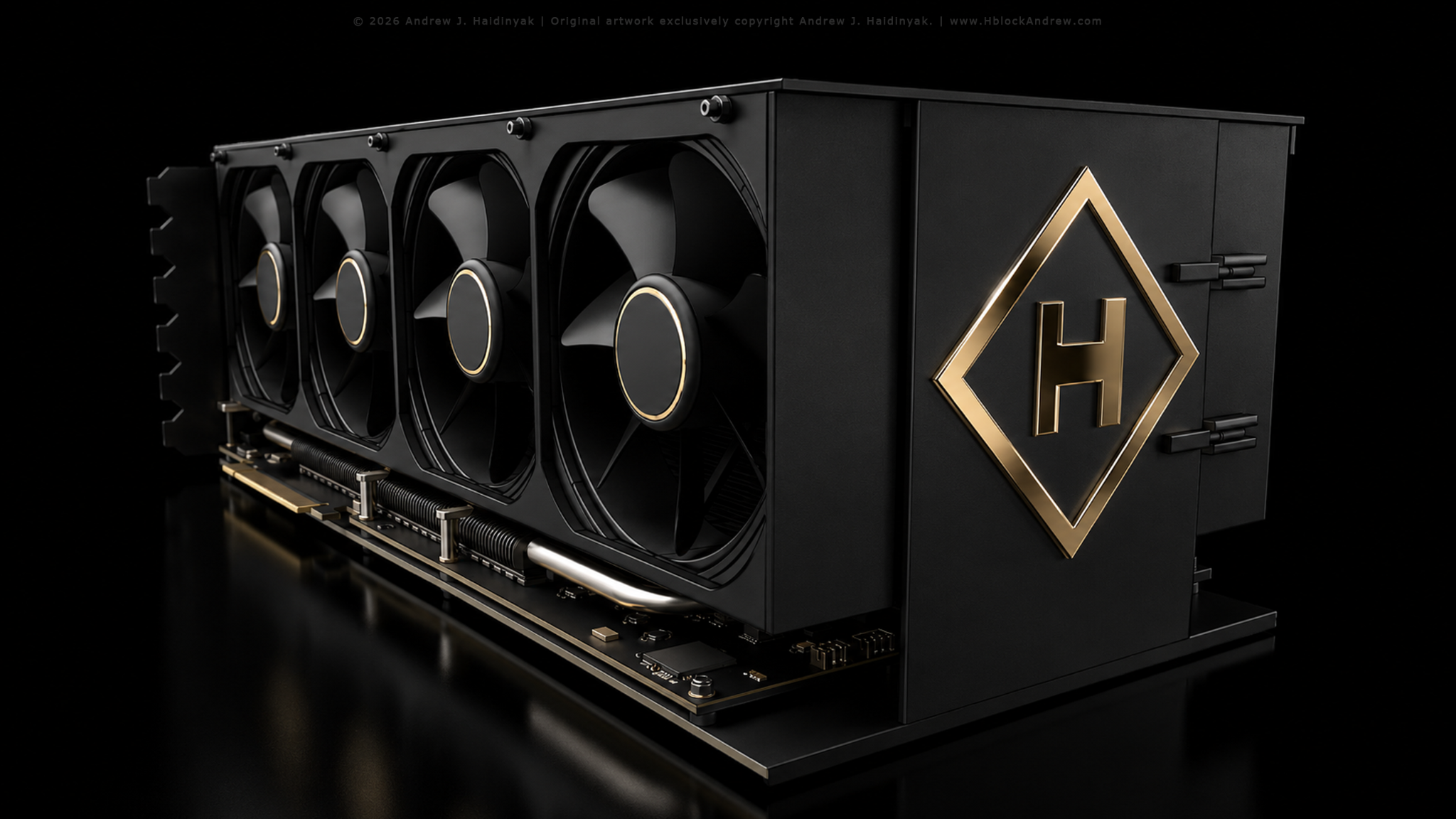
If NVIDIA or Valve ever examines the PHAETON Strike Cruiser-class architecture seriously, this document gives them more than a product sketch. It provides a strategic proposal and a clear record of how far I was willing to take the idea on my own.
I have only been working seriously with AI for about a year, and it has changed my life. For me, it has become one of the greatest teachers and learning tools I have ever had access to—especially for improving communication, organizing complex ideas, and learning how to write with purpose.
AI can take extremely complex ideas and help organize them into structures that are easier to test, question, and communicate. But the tool does not replace the person using it. The user still has to recognize the problem, supply direction, challenge bad reasoning, and sometimes see possibilities the AI itself does not recognize. To me, that is a testament to the human ability to reach beyond the tool.
I would be more than willing to work with experienced, team-oriented people who could give me greater access to the knowledge, tools, hardware, and development environment required to build at a higher level.
I am not presenting PHAETON because I expect every idea in this document to be accepted exactly as written.
I am presenting it because this is the level at which I intend to think, design, and build.